
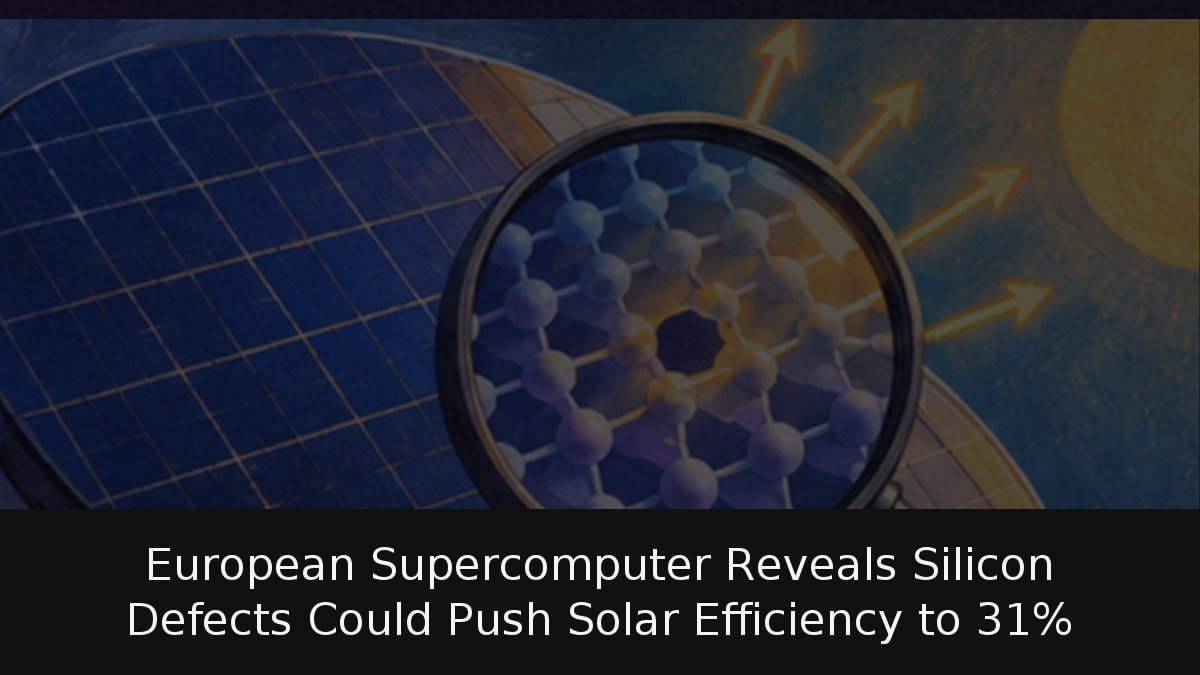
For decades, solar cell engineers have treated imperfections in silicon as a flaw to be engineered away. Now a research team at the University of Paderborn in Germany has found that one class of those imperfections may be doing useful work instead. Running first-principles quantum simulations on the Hawk supercomputer at the HLRS computing centre in Stuttgart — one of the most powerful machines in Europe — the researchers studied the interface between silicon and the organic semiconductor tetracene, and found that so-called dangling bonds actively assist the transfer of energy from the organic layer into the silicon. The findings, published in Physical Review Letters, question a design orthodoxy that has shaped photovoltaic research for decades.
- The discovery: Dangling bonds at a silicon–tetracene interface act as a bridge that enables singlet fission, letting one high-energy photon generate two electrons instead of one.
- The numbers: Today’s panels convert roughly 22% of incident sunlight. The team estimates a consistent singlet fission mechanism could lift hybrid tetracene-silicon cells to about 31%, a factor of 1.4.
- The catch: Tetracene degrades faster than silicon under prolonged sunlight, and depositing a uniform organic layer at industrial scale remains an unsolved manufacturing problem.
- Why it matters: Silicon still dominates around 95% of the solar market, so an efficiency gain here would touch the installed base worldwide rather than a niche technology.
Singlet fission: turning a heat loss into a second electron
The mechanism at the heart of the work is singlet fission. When a high-energy photon strikes tetracene, the excess energy above the roughly 1.1 eV that silicon can convert — around 3 eV in total — is normally wasted as heat. Singlet fission instead allows that single photon to spawn two lower-energy triplet excited states, which are then handed over to the silicon to produce two electrons rather than one.
What the Paderborn simulation adds is the missing link in that chain. The dangling bonds — silicon atoms at material interfaces that are not fully bonded to their neighbours — appear to be the bridge that makes the energy transfer efficient. The work was led by Dr. Marvin Krenz and coordinated by professor Wolf Gero Schmidt. In conventional solar design, these same imperfections are treated as traps that capture the electrons light has just created, which is why they have traditionally been eliminated rather than exploited.
Why the Hawk supercomputer was indispensable
Modelling the quantum behaviour of a silicon–tetracene interface at the scale of a real device demands millions of calculations for every picosecond of system evolution. The team relied on first-principles methods, which derive electronic properties directly from quantum equations without empirical approximations — an approach that is computationally prohibitive on conventional hardware. That is precisely the workload the Hawk machine at HLRS was built for.
The payoff, if the mechanism can be reproduced reliably, would be substantial. The professor’s estimate of a 1.4x efficiency factor would move hybrid tetracene-silicon cells toward a theoretical 31%. For context, solar efficiency has climbed by roughly 1% per year over the past two decades, and every additional percentage point in this field typically demands enormous research and development spending.
From laboratory result to production line
The gap between a promising simulation and a factory floor is the familiar obstacle for next-generation photovoltaics, and this case carries two extra technical challenges. First, tetracene is an organic material that degrades more quickly than silicon under sustained solar exposure, making long-term stability of the organic layer a genuine barrier. Second, depositing a homogeneous tetracene film on silicon at industrial scale without introducing other defect types that do suppress efficiency is a manufacturing engineering problem that nobody has solved yet.
Parallel work on the rival perovskite route shows how central defect control has become across the field. A team at the University of California San Diego, working with Princeton University and Sungkyunkwan University, used a temporary eutectic liquid formed by zinc bromide and methylammonium chloride to grow larger, more ordered perovskite crystals with fewer grain-boundary defects. Their devices reached efficiencies of roughly 24% to 26% and retained most of their performance after eight weeks of continuous operation under simulated sunlight, with the results published in Science.
“Perovskites made with the eutectic-forming additives had the longest lasting electron-hole pairs ever reported for any direct-bandgap semiconductor, which speaks to the promise of this approach.”
The remark came from study co-first author Connor Dolan, a chemical and nano engineering PhD alumnus. His team’s approach and the Paderborn result point in the same direction: better solar cells may come not from abandoning today’s materials, but from understanding their imperfections more precisely.
That distinction matters commercially. Perovskites are attractive because they can be processed from solution into thin films, potentially enabling cheaper, lower-energy manufacturing, but they still must prove durability at panel scale. Silicon, by contrast, already carries the global installed base. If dangling-bond-mediated singlet fission can be replicated in production, the gain would not be confined to a laboratory curiosity — it would apply to the material that overwhelmingly powers the world’s solar capacity today. The near-term research agenda is clear: stabilise the organic layer, control its deposition, and test whether a quantum effect observed on a supercomputer survives contact with a real manufacturing line.